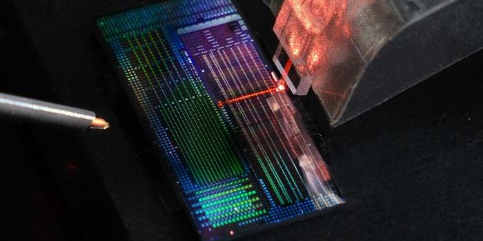
Graphene has been dubbed the "miracle material" because for its unique qualities and for a long time scientists have been working to use graphene for the production of nanoscale electronics. Graphene is ultra-thin -- only one atom thick and therefore two-dimensional making it excellent for conducting electrical current and ideal for future forms of electronics. However, because graphene is only one atom thick, any irregularities in the pattern can destroy its properties.
"Graphene is a fantastic material, which I think will play a crucial role in making new nanoscale electronics. The problem is that it is extremely difficult to engineer the electrical properties," says Peter Bøggild, a professor at DTU Physics. "When you make patterns in a material like graphene, you do so in order to change its properties in a controlled way -- to match your design. However, what we have seen throughout the years is that we can make the holes, but not without introducing so much disorder and contamination that it no longer behaves like graphene. It is a bit similar to making a water pipe, with a poor flow rate because of coarse manufacturing. On the outside, it might look fine. For electronics, that is obviously disastrous.”
Learn more about Graphene:
The Center for Nanostructured Graphene at DTU and Aalborg University was established in 2012 specifically to study how the properties of graphene can be engineered, for instance by making a very fine pattern of holes. This should subtly change the quantum nature of the electrons in the material, and allow the properties of graphene to be tailored. However, the team of researchers from DTU and Aalborg experienced the same as many other researchers worldwide: it didn't work.
To solve the graphene problem, a team of researchers at the Center for Nanostructured Graphene at DTU and Aalborg University have encapsulated graphene inside another two-dimensional material -- hexagonal boron nitride which is non-conductive material and is often used for protecting the properties of graphene. "We have shown that we can control graphene's band structure and design how it should behave. When we control the band structure, we have access to all of graphene's properties -- and we found to our surprise that some of the most subtle quantum electronic effects survive the dense patterning -- that is extremely encouraging. Our work suggests that we can sit in front of the computer and design components and devices -- or dream up something entirely new -- and then go to the laboratory and realise them in practice," says Peter Bøggild. "Many scientists had long since abandoned attempting nanolithography in graphene on this scale, and it is quite a pity since nanostructuring is a crucial tool for exploiting the most exciting features of graphene electronics and photonics. Now we have figured out how it can be done; one could say that the curse is lifted. There are other challenges, but the fact that we can tailor electronic properties of graphene is a big step towards creating new electronics with extremely small dimensions.”
Source: Technical University of Denmark