A recent study published in Nature examines the development of “multielement ink”, which is being touted as a new material for manufacturing semiconductors, which is the most essential component in computing, for both software and hardware. This study was conducted by a team of researchers at the University of California at Berkeley and holds the potential to help improve semiconductor manufacturing processes, including the reduction of energy required for it.
“The traditional way of making semiconductor devices is energy-intensive and one of the major sources of carbon emissions,” said Dr. Peidong Yang, who is a professor of chemistry and materials science and engineering at UC Berkeley and a co-author on the study. “Our new method of making semiconductors could pave the way for a more sustainable semiconductor industry.”
For the study, the team developed what they are referring to as high-entropy “multielement ink” halide perovskite which they discovered can be produced at room temperature, or even lower temperatures. This contrasts with the longstanding processes for semiconductors, which require temperatures as high as 2,700 degrees Fahrenheit (1,482 degrees Celsius). What makes this new ink so profound is it’s the first time researchers have attempted to use high-entropy materials to produce semiconducting materials capable of self-assembling with little energy input required, which is something researchers have been wanting to accomplish for years. Armed with this new ink, the researchers produced single-crystal semiconductors in much faster time that traditional semiconductor manufacturing methods.
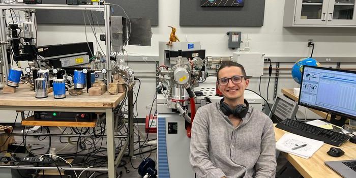
“Our high-entropy halide-perovskite semiconductor crystals, with their room-temperature and low-temperature methods, can be incorporated into an electronic device without destroying the other necessary layers, thus allowing for easier design of electronic devices and for more widespread use of high-entropy materials in electronic devices,” said Dr. Maria Folgueras, who is a Senior Research Scientist at Dow, a former PhD student of Dr. Yang, and lead author of the study.
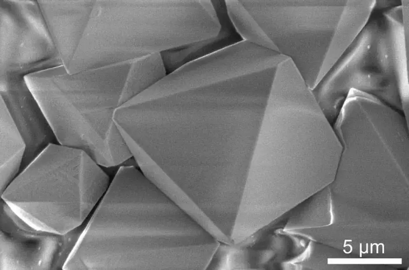
Image of six-element single crystals under a scanning electron microscope. The crystals are produced from the use of “multielement ink,” the first high-entropy semiconductor that can be manufactured at room temperature or even lower temperatures. (Credit: Maria Folgueras and Peidong Yang/Berkeley Lab. Image courtesy of Nature)
Potential applications for the new ink include lighting devices solid-state or color-tunable LEDs or waste heat recovery. In terms of computing, the new ink can also be used as a programming component that uses light to move or keep data.
How will this new ink help in semiconductor manufacturing in the coming years and decades? Only time will tell, and this is why we science!
As always, keep doing science & keep looking up!
Sources: Nature, EurekAlert!, Berkeley Lab