
Neuroscience
Is There a Genetic Component to Facial Recognition Skills?
JAN 10, 2014 12:00 AM PST
Share
Next-Generation Memory and Data Storage Technology
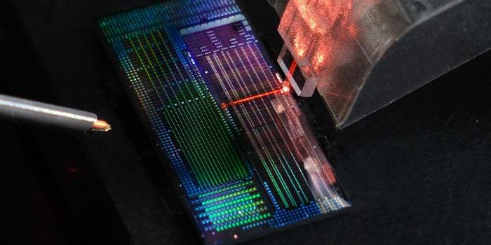
 Magnetoresistive Random Access Memory (MRAM) is a potentially revolutionary technology in the manufacturing of microelectronic devices. It stores information by using electron spin through creation of tiny magnetic fields at junctions in a two-dimensional array.
 MRAM effectively acts like a static random access memory chip (SRAM), except that it is non-volatile memory (retaining data even when the power is off). This technology can replace multiple kinds of memory (such as DRAM and flash) within an electronic device, providing an instant-on architecture for less cost, and generally consumes less power to operate. It also has one other advantage-it is unaffected by high radiation levels and extreme temperatures, making it extremely useful for space and defense applications.
Why isn't this technology already in use? It's already in use in limited ways-Freescale began selling commercial MRAM in 2006. But as with all new technologies, there are significant manufacturing challenges to overcome, as well as optimization of the type of technology. To reach universal acceptance, the density must be improved, manufacturing costs for the MRAM modules themselves must be lowered, and the memory retention time must increase.
One of the larger manufacturing challenges is the yield of the basic MRAM array structure. With a thickness of less than 1 nanometer (nm), the ferromagnetic structures are difficult to fabricate without significant yield losses, and the structure itself typically can only retain information for approximately 1 year. A research team at the National University of Singapore (NUS), collaborating with KAUST (King Abdullah University of Science in Technology) in Thuwal, Saudi Arabia, has developed a new method to address these concerns.
Instead of relying on a horizontal structure, the NUS team went with a multi-layered approach. By switching to a multilayer structure, the team was able to incorporate layers as thick as 20 nm, providing a more robust performance. The team expects that when using this technology, stored data can be retained for up to 20 years or more, with cheaper manufacturing costs. A summary of their work was published in the December 9th online version of Physical Review Letters.
The next step is to partner with chip manufacturers to test the technology in next generation real-world memory cell applications. Next generation variations of MRAM include Magneto-Transfer MRAM (M-T MRAM), which lowers power consumption by combining magnetic fields and heating from pulse currents to write the data; and Vertical Transport MRAM (VMRAM), which focuses on density reduction by using current perpendicular to the plane for switching purposes.
The NUS team is hunting for a partner using a spin-orbit torque transfer MRAM architecture (where the electron spin used for storage is achieved by direct application of current instead of through induction of a magnetic field). In this field, power consumption is reduced through reducing the write currents necessary to produce data.
With this effort and others that are focused on robust manufacturing and improvement of the MRAM architecture, it's likely you will see these modules take over in computers, cell phones, and other mass-produced microelectronic devices sometime in the next decade.

Bachelor's (BA/BS/Other)
You May Also Like
OCT 30, 2025
Technology

How can text messages improve hospital discharges and post-discharge quality? This is what a recent study published in t
...
DEC 12, 2025
Technology
How can a computer chip the size of a human hair enhance the future of quantum computing? This is what a recent study pu
...
DEC 16, 2025
Earth & The Environment

How can an aircraft’s contrails, which are artificial ice clouds formed from hot engines and cold altitudes, contr
...
JAN 06, 2026
Space & Astronomy

Are Sun-like stars the only stars where Earth-like worlds exist? This is what a recent study presented this morning at t
...
JAN 08, 2026
Earth & The Environment
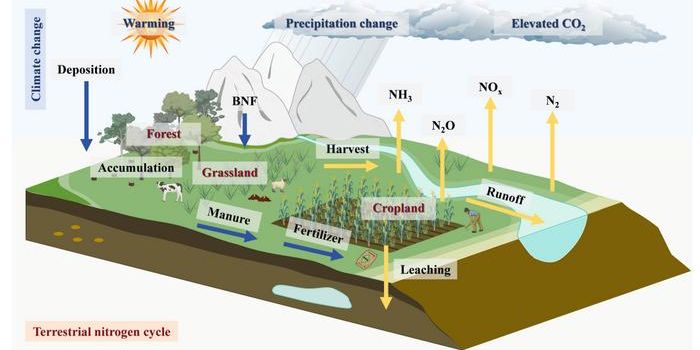
How does climate change influence the planet’s nitrogen cycle? This is what a recent study published in Nitrogen C
...
JAN 15, 2026
Cardiology

Your future health outcomes may be predictable using AI and a recording of your sleep.
Loading Comments...